- 您现在的位置:买卖IC网 > Sheet目录342 > MCP14E6T-E/MF (Microchip Technology)IC MOSFET DRIVER 2A 8DFN-S
�� ��
��
��MCP14E6/7/8�
�3.0�
�PIN� DESCRIPTIONS�
�The� descriptions� of� the� pins� are� listed� in� Table� 3-1� .�
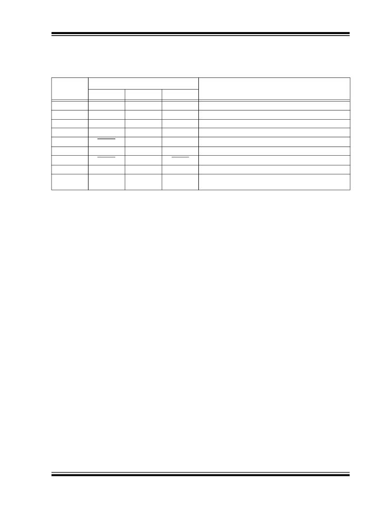
�TABLE� 3-1:�
�PIN� FUNCTION� TABLE�
�PDIP,� SOIC,�
�6x5� DFN�
�1�
�2�
�3�
�4�
�5�
�6�
�7�
�8�
�9�
�MCP14E6�
�ENB_A�
�IN� A�
�GND�
�IN� B�
�OUT� B�
�V� DD�
�OUT� A�
�ENB_B�
�EP�
�Symbol�
�MCP14E7�
�ENB_A�
�IN� A�
�GND�
�IN� B�
�OUT� B�
�V� DD�
�OUT� A�
�ENB_B�
�EP�
�MCP14E8�
�ENB_A�
�IN� A�
�GND�
�IN� B�
�OUT� B�
�V� DD�
�OUT� A�
�ENB_B�
�EP�
�Description�
�Ouptut� A� Enable�
�Input� A�
�Ground�
�Input� B�
�Output� B�
�Supply� Input�
�Output� A�
�Output� B� Enable�
�Exposed� Metal� Pad� (� DFN� package� only� ).� Exposed� pad� is�
�electrically� isolated.�
�3.1�
�Enable� A� (ENB_A)�
�3.5�
�Supply� Input� (V� DD� )�
�The� ENB_A� pin� is� the� enable� control� for� Output� A.� This�
�enable� pin� is� internally� pulled� up� to� V� DD� for� active-high�
�operation� and� can� be� left� floating� for� standard� opera-�
�tion.� When� the� ENB_A� pin� is� pulled� below� the� enable�
�pin,� Low� Level� Input� Voltage� (V� EN_L� ),� Output� A� will� be�
�in� the� OFF� state,� regardless� of� the� input� pin� state.�
�V� DD� is� the� bias� supply� input� for� the� MOSFET� driver� and�
�has� a� voltage� range� of� 4.5V� to� 18V.� This� input� must� be�
�decoupled� to� ground� with� a� local� ceramic� capacitor.�
�This� bypass� capacitor� provides� a� localized� low-�
�impedance� path� for� the� peak� currents� that� are� provided�
�to� the� load.�
�3.2�
�Control� Inputs� A� and� B� (IN� A;� IN� B)�
�3.6�
�Enable� B� (ENB_B)�
�The� MOSFET� driver� inputs� are� a� high-impedance�
�TTL/CMOS� compatible� input.� The� inputs� also� have�
�hysteresis� between� the� high� and� low� input� levels,�
�allowing� them� to� be� driven� from� slow� rising� and� falling�
�signals,� and� to� provide� noise� immunity.�
�3.3� Ground� (GND)�
�Ground� is� the� device� return� pin.� The� ground� pin� should�
�have� a� low-impedance� connection� to� the� bias� supply�
�source� return.� High� peak� currents� will� flow� out� the�
�ground� pin� when� the� capacitive� load� is� being�
�discharged.�
�The� ENB_B� pin� is� the� enable� control� for� Output� B.� This�
�enable� pin� is� internally� pulled� up� to� V� DD� for� active-high�
�operation,� and� can� be� left� floating� for� standard� opera-�
�tion.� When� the� ENB_B� pin� is� pulled� below� the� enable�
�pin,� Low-Level� Input� Voltage� (V� EN_L� ),� Output� B� will� be�
�in� the� OFF� state,� regardless� of� the� input� pin� state.�
�3.7� Exposed� Metal� Pad� (EP)�
�The� exposed� metal� pad� of� the� DFN� package� is� not�
�internally� connected� to� any� potential.� Therefore,� this�
�pad� can� be� connected� to� a� ground� plane,� or� other� cop-�
�per� plane� on� a� printed� circuit� board,� to� aid� in� heat�
�removal� from� the� package.�
�3.4�
�Outputs� A� and� B� (OUT� A;� OUT� B)�
�Outputs,� A� and� B,� are� CMOS� push-pull� outputs� that� are�
�capable� of� sourcing� and� sinking� 2.0A� of� peak� current�
�(V� DD� =� 18V).� The� low� output� impedance� ensures� the�
�gate� of� the� MOSFET� will� stay� in� the� intended� state,�
�even� during� large� transients.�
�?� 2011� Microchip� Technology� Inc.�
�DS25006A-page� 11�
�发布紧急采购,3分钟左右您将得到回复。
相关PDF资料
MCP14E9T-E/MF
IC MOSFET DRIVER 3A 8DFN-S
MCP1640RD-4ABC
BOARD REF DES AAAA BAT BOOST
MCP3906AT-E/SS
IC ENERGY METERING 24SSOP
MCP3907T-I/SS
IC ENERGY METER W/OSC 24SSOP
MCZ33198EF
IC TMOS DRIVER AUTO HISIDE 8SOIC
MCZ33285EFR2
IC TMOS DRIVER DUAL HISIDE 8SOIC
MCZ33927EK
IC FET PRE-DRIVER 3PH 54-SOIC
MCZ33937EKR2
IC PRE-DRIVER 3PHASE 54-SOIC
相关代理商/技术参数
MCP14E6T-E/SN
功能描述:功率驱动器IC 3A MOSFET Driver RoHS:否 制造商:Micrel 产品:MOSFET Gate Drivers 类型:Low Cost High or Low Side MOSFET Driver 上升时间: 下降时间: 电源电压-最大:30 V 电源电压-最小:2.75 V 电源电流: 最大功率耗散: 最大工作温度:+ 85 C 安装风格:SMD/SMT 封装 / 箱体:SOIC-8 封装:Tube
MCP14E7
制造商:MICROCHIP 制造商全称:Microchip Technology 功能描述:2.0A Dual High-Speed Power MOSFET Driver With Enable
MCP14E7-E/MF
功能描述:功率驱动器IC 3A MOSFET Driver RoHS:否 制造商:Micrel 产品:MOSFET Gate Drivers 类型:Low Cost High or Low Side MOSFET Driver 上升时间: 下降时间: 电源电压-最大:30 V 电源电压-最小:2.75 V 电源电流: 最大功率耗散: 最大工作温度:+ 85 C 安装风格:SMD/SMT 封装 / 箱体:SOIC-8 封装:Tube
MCP14E7-E/MF
制造商:Microchip Technology Inc 功能描述:; Peak Reflow Compatible (260 C):Yes; Le
MCP14E7-E/P
功能描述:功率驱动器IC 3A MOSFET Driver RoHS:否 制造商:Micrel 产品:MOSFET Gate Drivers 类型:Low Cost High or Low Side MOSFET Driver 上升时间: 下降时间: 电源电压-最大:30 V 电源电压-最小:2.75 V 电源电流: 最大功率耗散: 最大工作温度:+ 85 C 安装风格:SMD/SMT 封装 / 箱体:SOIC-8 封装:Tube
MCP14E7-E/P
制造商:Microchip Technology Inc 功能描述:; Peak Reflow Compatible (260 C):Yes; Le 制造商:Microchip Technology Inc 功能描述:IC, MOSFET DRVR, DIP-8
MCP14E7-E/SN
功能描述:功率驱动器IC 3A MOSFET Driver RoHS:否 制造商:Micrel 产品:MOSFET Gate Drivers 类型:Low Cost High or Low Side MOSFET Driver 上升时间: 下降时间: 电源电压-最大:30 V 电源电压-最小:2.75 V 电源电流: 最大功率耗散: 最大工作温度:+ 85 C 安装风格:SMD/SMT 封装 / 箱体:SOIC-8 封装:Tube
MCP14E7-E/SN
制造商:Microchip Technology Inc 功能描述:; Peak Reflow Compatible (260 C):Yes; Le 制造商:Microchip Technology Inc 功能描述:IC, MOSFET DRVR, SOIC-8